X-ray imaging sees chip defects
Real-time x-ray inspection system explores ICs for hidden solder and wiring flaws and defective printed-circuit-board connections.
By R. Winn Hardin, Contributing Editor
Chip-scale packages (CSPs) are now just slightly larger than the die-and-lead frame that they hermetically enclose. This advanced packaging system for integrated circuits (ICs) includes ball-grid-array (BGA) and column-grid-array (CGA) packages. To accommodate the hundreds of I/O ports on current ICs, connectors are fastened to the bottom of the chip, with solder balls or columns connecting the underside of the printed wiring assembly. Because the connections join the IC and the underlying board, automated-optical-inspection equipment is able to inspect the attached ICs.
Like many OEM suppliers, SoPark Corp. (Buffalo, NY, USA), a contract electronics manufacturer with a broad product mix, has had to adapt its manufacturing lines to include CSP components. To accomplish that changeover, SoPark turned to YESTech Inc. (San Clemente, CA, USA) to provide an inspection system that would improve the BGA attachment process and reduce board rework.
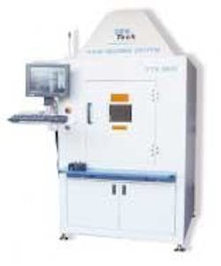
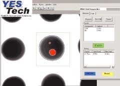
YESTech provides the YTX-3000 high-resolution, real-time x-ray inspection system with a programmable stage, x-ray source, PC, and image intensifier coupled to a medium-resolution CCD camera for high-contrast imaging (see photo). This off-line inspection system images hidden solder contacts beneath the BGA components, after attachment, to help achieve 100% inspection and to refine soldering and attach manufacturing processes to limit the amount of board rework required by defective connections (see Fig. 1).
Process enhancement
"Initially, SoPark was looking to the YTX-3000 mainly to detect faulty boards, but, over time, the plan is to gain quantitative process information so that the company can move from detection to prevention," notes Don Miller, president and cofounder of YESTech. "With x-rays, you get a feel for the capabilities of your process, and, from there, you dig down to the next level and say, 'If I run it at this temperature or ramp rate, I can get better results.' You then fine-tune the process to improve yields."
"We did an extensive review of x-ray systems, and the YESTech YTX-3000 proved best at meeting our current and future needs," says SoPark engineering manager David Ratajczak. "It has the same features as do more expensive machines. It will be a valuable tool in helping us improve our BGA assembly process. We are already seeing positive responses from our customers."
YESTech director of manufacturing Bob Lin adds, "YTX-3000 allows YesTech to quantify the process in relation to voids, which could not be measured previously. For some product mixes, manufacturers use the YTX system on 100% of the product going out the door. For others, they inspect one out of 20—it's customer specific."
Says YESTech's Miller, "The system we sold for $120,000 in the past we're selling for $80,000 today, with resolution of 5 µm rather than 10 to 15 µm for the older systems. Better sensitivity of the camera and image-intensifier systems is helping us to get that performance," Miller adds.
X-ray tubes
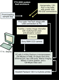
The YTX-3000 system uses a stationary Hamamatsu Corp. (Bridgewater, NJ, USA) 130-KeV microfocus x-ray tube as the illumination source. YESTech's Lin chose this tube because it has three remotely selectable spot-size widths—5, 10, and 30 µm—that allow for wide power load and high-resolution imaging. The beam width is controlled by the PC host via an RS-232 interface. "We're working with Hamamatsu to go to the USB standard," Lin says, "but they're not there yet." YESTech uses USB 2.1 interfaces between most system components; its future systems will use this format exclusively because of its high bandwidth and the ease of establishing network connections with inexpensive USB electronics.
When used with a Toshiba (Irvine, CA, USA) J-series image intensifier with its large output aperture 20-mm output-phosphor screen, the Hamamatsu x-ray tube enables the x-ray imaging system to achieve crisp images at 5-mm resolution. The J-series includes a multichannel amplifier plate to collect the x-rays that are not absorbed as they pass through the board under test. The x-rays create an electron flow in the multichannel plate that impacts the phosphor screen and causes the screen to emit light with an intensity relative to the strength of the x-rays.
Lin says, "Others have similar products, but Toshiba's product provides a higher resolution. The output phosphor screen is large for this type of application. Other x-ray inspection machines use 10- or 15-mm phosphor screens. The only thing that would give us better resolution is a flat-panel detector, which is expensive and not practical for many assembly applications," he adds.
A Sony Electronics (Park Ridge, NJ, USA) XCES51 1/2-in. black-and-white CCD camera with a sensitivity of 0.2 lux at f/1.4 is C-mounted to the intensifier output. High sensitivity is important here because x-ray images are essentially shadowgraphs with a 256-bit gray-scale depth after digitization. Greater sensitivity means higher contrast and sharper images, according to Lin.
The Sony camera is triggered through an RS170 interface by a Matrox Imaging (Dorval, QC, Canada) Meteor II frame grabber and returns a 768 × 494-pixel image to an A/D converter. A bitmap image with a 256-bit gray-scale depth is ported across the PCI bus into the PC's resident memory, where YESTech's proprietary software performs image processing.
According to Lin, YESTech selects generic, cutting-edge desktop PCs. "We've mounted the PC below the x-ray enclosure so that it can be easily swapped out for a new system for upgrade or repair. We don't need an industrialized PC because the there's not much chance of dropping the heavy YTX system. We've gone down the path that gives the best performance at the best price," Lin explains.
Systems are now shipped with a Pentium-4, 2.4-GHz microprocessor, 248 Mbytes of RAM, a 20- or 40-Gbyte hard drive, Ethernet capability, a 128-Mbyte generic video card with digital output, a 17-in. flat screen for the high-resolution display of images at 1200 × 1024 pixels, a DVD ROM drive, and either a Hewlett-Packard (HP; Palo Alto, CA, USA) 130 photo printer or a larger Sony 5500 video printer.
"DVD is our future," says Lin. "CD burners are limited in size and are often misused by technicians. With a DVD, we can put a full system installation process with all the software on a single disk. You can't get that much information on a CD, especially with the page sizes of Windows XP. We suggest the use of HP 4 × 6 photo printers because they are economical. The images are mostly printed so they can be copied, stored, or thrown away. It's $0.10 a print versus $1 with a larger printer." When printing is not necessary, Lin adds that the system's Ethernet capability allows stored images to be accessed from anywhere within the company's local-area network.
X-ray magnification
The system PC also controls a proprietary four-axis stage designed by YESTech. This stage allows 15-in. travel along the y-axis, 20 in. along the x-axis, 18 in. along the z-axis, and 360° rotation along the x-axis. Geometric magnification of up to 48x is achieved by moving the stage and the board under test closer to the x-ray source at a 5-µm beam width. Upcoming versions of the YTX system will use a rotating stage with a moveable x-ray tube source to provide 3-D shadowgraphs similar to those obtained by computed-tomography systems (see Fig. 2). The stage connects to the PC through a USB connection.
During operation, the technician loads a board or tray of CSP ICs, depending on the application, into the system's lead enclosure. The technician starts the inspection process, which initiates a stored macro function that is specific to the board under inspection and directs the camera to acquire a wide-angle image of the board under test. The YESTech software uses a pixel-to-pixel comparison to a stored "golden part" template to find metal fiducials on the printed-wiring-assembly board and to align the stage to the correct region of interest (ROI), such as an attached BGA. The imaging system then switches the x-ray beam width to the appropriate setting (5 µm for the highest resolution), and the camera acquires an image of the ROI.
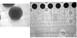
From this point, the macro function performs preprogrammed inspection processes, such as identifying voids, locating voids, and measuring the total area of voids (see Fig. 3). "The macro recorder works like a VCR," Lin says. Images or pass/fail data can be displayed on the flat-screen monitor, depending on the application.
For SoPark, pass/fail, location, and other data are put into Microsoft Excel format and stored locally on the hard drive or transmitted across the LAN to a central server. This storage technique is the one potential bottleneck in the system, according to Lin. "An inspection takes about 1 s to display. That's what users want, immediate results. The only thing that can slow it down is saving an image file to a server if the network is slow," he adds.
Future designs
YESTech is working on the next-generation YTX system. Lin's design team is building a new camera that uses a 1.3-Mpixel black-and-white CCD chip from Philips Semiconductor (Sunnyvale, CA, USA) to improve system resolution. YESTech's Miller claims that the new camera with a USB connector and onboard A/D converter will cost one-third the price of an available camera. The company is also developing a color camera that combines automated optical inspection and x-ray imaging into one inspection process. Next-generation systems will also make use of the four-axis rotational stage to perform tomography and laminography imaging of PWA and CSP assemblies.
Company Info
Hamamatsu Corp. www.hamamatsu.com
Hewlett-Packard Co. www.hewlett-packard.com
Matrox Imaging www.matrox.com/imaging
Philips Semiconductor www.semiconductors.philips.com
Sony Electronics www.sony.com/videocameras
SoPark Corp. www.sopark.com
Toshiba America Electronic Components Inc. www.toshiba.com/taec
YESTech Inc. www.yestechinc.com