Frame grabber aids semiconductor milling
Frame grabber enables production of enhanced real-time images from a focused ion-beam device for microcircuit editing of semiconductors.
By Joe Sgro
The increased accuracy and utility of an optical imaging focused-ion-beam (FIB) milling device in conjunction with a powerful frame-grabber board has been proven to save an entire debug/fabrication cycle of semiconductor circuit design. This integrated system can save manufacturing expenses of $1 million to $2 million and several weeks of production. FIB toolmakers are pursuing different approaches to the same goal and are introducing new designs. The results of such competition are expected to produce significant benefits for suppliers, customers, and end users.
New semiconductors are harder to design, test, and debug as a result of growing complexity, decreased feature size, and new materials and manufacturing processes. Moreover, in today's environment of continually shortening product life cycles, all of the phases of semiconductor design, testing, and debugging must be completed within extremely short schedules to prevent the new product from being virtually obsolete when brought to market.
Traditional semiconductor testing and debugging methods, which rely on testing a finished prototype and respinning it over and over until it functions as desired, as well as increasingly expensive mask sets and other materials can result in substantial added expenses and time-to-market delays. The debug stage typically finds both circuit logic errors and potential timing issues. Respinning a design to address these issues can cost months and millions of dollars. The best way to avoid such delays and expenses is to ensure that errors are detected and corrected in the initial prototype stage by rapidly micromachining the prototype, thereby obviating the need for expensive and time-consuming respins.
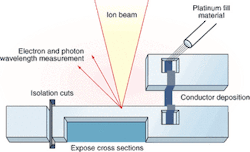
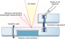
FIB technology has been the pre-eminent tool for microcircuit editing for almost a decade, and it has became the preferred microscopy sample-preparation tool for site-specific applications. This technology can both create and modify microstructures by using its precision capabilities to remove material, deposit material, and provide localized ion implantation (see Fig. 1). It also can image the sample via secondary electrons or ions before, after, and during micromilling. The ability to image while removing or depositing material provides important feedback for process control.
The challenge
Silicon micromachining consists of modifying a circuit by cutting interconnects in the chip, with FIB milling and forming other interconnects with FIB metal deposition. The interconnections are within the active layer of the silicon, sandwiched between the package and bulk silicon. Therefore, circuit modification begins with the removal of silicon to access the active layers of the chip and ends with FIB micromachining.
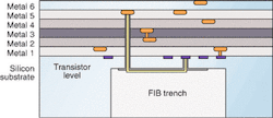
FIB interconnections commonly are made to metal lines, but must avoid milling transistors or other lines (see Fig. 2). This restriction places a severe width constraint on the vias made by FIB. Multiple metal layers incorporating new materials (such as dielectric films and silicon-on-insulator (SOI), both of which are sensitive to invasive charged particles and advanced packaging techniques (such as flip-chip), have severely compounded the problem. At the same time, the width of the gate structure in transistors is rapidly shrinking to less than 0.09 µm, rendering traditional circuit-editing techniques obsolete. For example, to reach Metal 1 and initiate editing and milling with standard FIB tools, the average time is eight hours, according to officials at NPTest (San Jose, CA, USA).
FIB coals
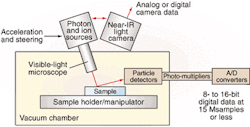
Using the standard FIB approach efficiently in conjunction with the newer semiconductor feature sizes, complexity, and layouts must achieve precise beam placement, must eliminate semiconductor movement, and must ensure imaging to 0.1-µm accuracy. Accordingly, NPTest developed the IDS OptiFIB that integrates an optical and ion microscope in a single, coaxial tube that operate simultaneously during circuit analysis and editing following first silicon (see Fig. 3). This helps reduce milling time from hours to minutes, claims NPTest officials.
The OptiFIB device can edit from the front or backside of a wafer, regardless of the material used in the IC stack employing the integrated microscopes. It features in situ alignment, combining ion and photon optical microscopes in a coaxial photon ion microscope to support front-side and backside milling using through-silicon imaging.
Viewing the real-time optical image through silicon during the ion-beam editing process accommodates accurate end pointing to stop milling. As a result, the imaging system can perform edits on any manufacturing process technology, including SOI, low-k, and copper. Because the OptiFIB can edit circuits from the front or backside and its optical microscope provides noninvasive, infrared imaging, it can use optical end pointing during the milling process. This approach skips several traditional steps in FIB editing, such as creating fiducial trenches. These features also increase throughput and accuracy, because the OptiFIB can navigate to the first metal layer in about 30 minutes. The optical imaging can also see through low-k dielectric materials and silicon-on-insulator, as well as silicon, allowing backside editing of circuits. This is because all of a chip's signals are routed through the initial metal layer.
Optical navigation
The OptiFIB tool allows IC diagnostic engineers to etch and deposit metal while concurrently imaging safely on today's advanced devices. The OptiFIB system uses photons to enable noninvasive, through-silicon imaging, which results in optical images that can be used for accurate navigation. The coaxial column and photon optics allow the operator to see through silicon (including dielectrics and heavily doped silicon) to accurately align the FIB and computer-aided-design (CAD) images and simultaneously drill with precision. The CAD layout tool enables the operator to overlay the CAD with the optical and FIB images, ensuring 0.1-µm edit accuracy using a Sun Microsystems (Santa Clara, CA, USA) workstation (see Fig. 4).
Placement accuracy is achieved by making use of the subpixel resolution algorithm typically performed in advanced lithography. This algorithm provides a precise way to align CAD data and the optical image.
The OptiFIB device is easy to align and features achromatic imaging technology to maintain alignment. Achromatic imaging, using a set of mirror lenses instead of glass, eliminates image aberrations when moving from blue to infrared light. This feature of the coaxial column enhances image quality and real-time simultaneous imaging. Through-silicon navigation and imaging use the coaxial column to optically view editing locations while performing modifications. Furthermore, the operator can use software-driven, low-ion-current end-point detection to control the milling depth more accurately. An end-point analyzer detects changes in device material and prompts automated milling termination.
Signal acquisition
The position of the FIB beam is determined by a commercial x-y waveform generator, which can scan it with any path the designer of the system desires. In scanning systems it is normal to restrict the beam path to areas of interest for diagnostic measurements of both secondary electrons and x-rays for imaging. In FIB systems, the path of the beam can be used to remove or add material (as controlled by the focus and energy of the beam) and moves at a non-Cartesian slow rate.
Therefore, a FIB system presents several challenges to the data-acquisition interface boards. Often, these vision systems use custom interface boards, such as frame grabbers, to provide the functionality required. When using an off-the-shelf board, the range of pixel clock speeds must be extremely large, from 10 kHz to 10 MHz. To improve the performance of these systems, partial frames must be delivered so that the image can be developed as it is being scanned. Normal frame grabbers are "frame oriented"—that is, the data are provided when the frame is done.
Both FIB and SEM applications take advantage of the ability of the source to do nonraster scanning. Accordingly, the nonraster-oriented image must be converted to a raster-oriented image for display.
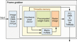
The FastFrame1300 frame grabber board from Alacron Inc. (Nashua, NH, USA) was found to meet these requirements (see Fig. 4). It contains a programmable input FPGA, which feeds directly into a TriMedia TM1300 image processor from Philips Semiconductors (Eindhoven, The Netherlands) that can be used to reformat the data. The half-length PCI frame grabber and the TriMedia processor can provide more than 720 MFLOPS.
Specifically, pixel values flow from the hardware in the order in which they are scanned. The pixel locations are provided to the frame grabber as x-y coordinates, which are not aligned to the desired raster pixels. The frame-grabber software precomputes a table that defines which pixels in the hardware data are used to compute the values of each pixel in the raster image. In other words, the raster image is derived from the hardware image.
The raster pixels are weighted sums of the hardware pixels. The weights for a raster pixel are computed from the values of the four nearest hardware pixels: above, below, left, and right of the raster pixel location. The actual conversion is done using the on-board TriMedia processor on the hardware pixels, and the raster and vector images are sent to the host. The raster image is displayed and the hardware image controls the system (focus, energy, and so forth, depending on the application).
The author acknowledges the contributions of Jim Siebert, staff systems engineer, and Lokesh Johri, software engineering manager, NPTest, San Jose, CA, USA.
JOE SGRO is chief executive officer, Alacron Inc., Nashua, NH, USA; www.alacron.com.
Company Info
Alacron Inc. www.alacron.com
NPTest www.nptest.com
Philips Semiconductors www.semiconductors.philips.com
Sun Microsystems www.sun.com
