Image sensor-processor bridge facilitates low-cost camera designs with microcontroller interfaces
Designers ofembedded imaging systems must develop systems that cost-effectively interface image sensors with low-cost image processors. However, since most image sensors produce image data at very high data rates, designers cannot easily interface the sensors with low-cost microcontrollers (MCUs); often no buffering is provided within the image sensors themselves and most MCUs have limited internal memory.
“Since manyimage-processing algorithms require random access to pixel data,” says Tareq Hasan Khan of the Multimedia Processing and Prototyping Laboratory at the University of Saskatchewan (Saskatoon, SK, Canada), “this lack of memory presents a problem for developers wishing to interface high-speed image sensors with low-cost microcontrollers such as Intel’s [Santa Clara, CA, USA] 8051.”
While high-speed image sensors can be interfaced to more advanced MCUs such as the AT91CAP7E from Atmel (San Jose, CA, USA), the additional features of those MCUs, such as peripheral DMA controllers and USB andFPGA interfaces, may not be required for simple, low-cost imaging applications.
Tareq Hasan Khan and Khan Wahid have developed a digital-video-port (DVP) compatible device designed to bridge any general-purpose image sensor with low-cost MCUs. The device, known as iBRIDGE, allows commercially available DVP-based CMOS image sensors—such as the TCM8230MD from Toshiba (Tokyo, Japan), OVM7690 from OmniVision (Santa Clara, CA, USA), MT9V011 from Aptina (San Jose, CA, USA), LM9618 from National Semiconductor (Santa Clara, CA, USA), KAC-9630 from Kodak (Rochester, NY, USA), and PO6030K from Pixelplus (Gyeonggi-do, Korea)—that use DVP to be interfaced to MCUs such as the 8051 and the PIC from Microchip Technology (Chandler, AZ, USA).
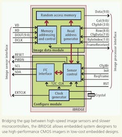
To allow these DVP-based image sensors to interface with slower, low-power MCUs, the iBRIDGE design features an image data module and a system configuration module (see figure). Since most standard-definition (SD) and high-definition (HD) CMOS image sensors transfer image data using the DVP interface, this is implemented in the iBRIDGE design. This interface uses the imager’s vertical sync (VD) and horizontal sync (HD) pins to indicate the end of frame and end of row, respectively while pixel data is transferred over DOUT.
Initialization and configuration of the image sensor is performed over the I2C protocol. This controls the imager’s frame size, color, and sleep and wakeup mode by using two wires to send serial data (SDA) and serial clock data (SCL) to the image sensor.
To configure and access image data, the processor provides both configuration signals and frame access signals. The configuration signals are asynchronous; frame access signals depend on the speed of the MCU and are not synchronized with the iBRIDGE’s internal clock. A single-port random access memory (RAM) module is used to store a frame of data from the DVP-compatible imager.
For evaluation, Khan modeled the iBRIDGE in VHDL and used the DE2 Development and Education board fromAltera (San Jose, CA, USA) to synthesize the design onto the board’s Cyclone II 2C35 FPGA. This FPGA was then interfaced to a TCM8230MD DVP-based CMOS imager from Toshiba and an ATmega644 MCU from Atmel. The MCU was interfaced to a PC using the COM port of the MCU and captured images displayed on the PC via software written in Visual Basic.
Using the bridge between high-performance image sensors running as fast as 254 MHz and low-speed MCUs running at 1 MHz, VGA images can be captured at up to 333 frames/s. Thus, by employing the iBRIDGE and low-cost MCU, any DVP-compatible commercial image sensor can be converted to a high-speed randomly accessible image sensor.
-- By Andrew Wilson,Vision Systems Design
