The worldwide semiconductor shortage that began in 2021 continues to shape the world. This has shocked industries as diverse as consumer electronics, transportation, defense, telecommunications, and even heavy industry. Automakers faced hobbled production schedules and consumer electronics companies delayed or even cancelled launches. According to a 2022 report,1 the shortage of semiconductors has caused manufacturing lead times to increase from an average of three to four months to 10-12 months.
Hundred-billion dollar revenue losses2 and missed opportunities mounted, drawing even more attention to one of our most important—but also unnoticed—industries. As markets and countries came to terms with the scope and causes of semiconductor production issues, they also started actively exploring solutions.
Investing in a Bigger Vision and Much Tinier Solutions
One of those solutions is investment. Multiple sources predict a semiconductor industry worth a trillion dollars by 2030, which would make it one of the top five industries in the world.3-4 Getting there will require a huge investment in infrastructure.
One factor in this growth will be renewed leadership in the American semiconductor industry. Today semiconductors manufactured in the United States account for only 12% of the global total. This is down from a high of 37% just 30 years ago.5 Even within that diminished contribution, most of it is not in leading-edge, small node size chips (those under 10 nanometers). The US government has decided that’s about to change, committing a huge new level of investment through the CHIPS and Science Act of 2022 to encourage research, investments in infrastructure and a robust supply chain.5
Huge investments in semiconductor manufacturing infrastructure will trickle down beyond the semiconductor fabrication plants (fabs) themselves to the many enabling equipment makers that make the chips possible. We expect that to include huge growth in the exposure systems and photolithography equipment used to fabricate semiconductors, as well as the inspection equipment used to evaluate key stages of the manufacturing process.
Related: OCR System Reads Codes on Semiconductor Wafers
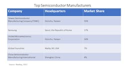
At the same time, the demand for innovation—smaller nodes and higher yields—will keep pace if not accelerate. That is no easy feat. While Moore’s observation is no longer the “Law” it once was, there is still rapid improvement happening. Fabs, like Taiwan Semiconductor Manufacturing Company (Hsinchu, Taiwan) are touting their competitiveness with ways to develop smaller node processes to reduce chip size and lower power consumption (while still increasing performance).6
The progression toward ever-smaller feature sizes and higher performance extends beyond the masks that define the circuit design all the way to the substrates that carry the integrated circuits, traces, switches, coatings, and other components to make up a printed circuit board. This means that even tiny imperfections can compromise signal integrity and more. Manufacturers keep uncovering new vulnerabilities, sensitivities, and defects as they push further toward—and beyond—nano-level production. The solution is lower tolerances at every step of the production cycle.
Imaging as a Key Enabler—And Challenge
In semiconductor manufacturing, yield is everything, driving output and costs. But lower tolerances and smaller components can be a huge challenge for inspection. Manufacturers looking at smaller geometries must manage yield with inspection at more points in the process, from wafer to finished PCB, so they can find defects sooner. The key is to continuously add more inspection steps without increasing the overall time for inspection. The imaging systems must provide higher resolution while reducing exposure period.
For integrated circuits, nanoscale features can become smaller than the visible or even UV wavelengths typically used. The precision needed to detect and quantify can approach the actual noise floor of sensors or even core operating principles. Solutions require new approaches, such as deep and extreme UV illumination and imaging. More and more precise imaging puts pressure on downstream components—the image processing hardware and software—that turn images into analysis for decision-making.
In PCBs, new levels of complexity in design and manufacturing has led to increasingly subtle material faults. Manufacturers need to detect a wide variety of defects, including breakage, abrasion, contamination, fragments and air bubbles. Traditional manual inspection or rule-based imaging may simply not be up to the task. Rule-based image processing techniques can struggle with reliability when dealing with PCB components that present high variations in shape, tone, contrast and texture. It then becomes impractical to build a robust inspection system with traditional algorithms. As a result, manufacturers have turned to AI functionality to supplement where traditional methods failed. AI algorithms can be trained on different samples of defective and non-defective PCB components to achieve a high degree of precision in classifying components.
Related: Fast Semiconductor Inspection with High Resolution Color Line Scan Cameras
Moving Past Conventional into Artificially Intelligent Imaging
One semiconductor OEM faced this challenge, leading to an increase in defective parts that went undetected in the company’s automated optical inspection (AOI) process. To solve the problem, the OEM implemented a new inspection solution combining both rule-based algorithms with AI functions for the AOI machine.
Using the AI software tools, the OEM achieved 98% accuracy in continual classification with 12-14 ms speed for 200 images and 100% accuracy with 453 good+ 11 bad images.
Additionally, the company was able to achieve 99.62% accuracy with 259 images and 20 ms speed for object detection when looking for multiple defects on a part image at the same time.
Getting Ready for 2030
McKinsey predicts that nearly 70% of growth in semiconductors3 over the next decade will be driven by just three industries: automotive, computation and data storage, and wireless communications. Each industry will be seeking further improvements in efficiency, performance, device size, and most importantly, scale. Imaging will be a key industry in getting them there.
References1. D Kaur. Chip Shortage: The Lack of “Chips to Make Chips” Is Exacerbating the Shortage by Another 2 Years. June 7, 202 Techwire Asia. https://techwireasia.com/2022/06/chip-shortage-the-lack-of-chips-to-make-chips-is-exacerbating-the-shortage-by-another-2-years/
2. M Placek. Projected revenue and production loss of the global automotive industry as a result of the semiconductor chip shortage in 2021. Statista, September 28, 2022. https://www.statista.com/statistics/1280639/automotive-industry-revenue-and-production-loss-forecast/
3. O Burkacky, J Dragon, N Lehmann. The global semiconductor industry is poised for a decade of growth and is projected to become a trillion-dollar industry by 2030. McKinsey & Company, April 1, 2022. https://www.mckinsey.com/industries/semiconductors/our-insights/the-semiconductor-decade-a-trillion-dollar-industry
4. M Hall. ISS 2022: Semiconductor industry market outlook and prospects for reaching $1 trillion by 2030. Semi, May 9, 2022. https://www.semi.org/en/blogs/business-markets/iss-2022-semiconductor-industry-outlook-and-prospects-for-reaching-%241-trillion-by-2030
5. Fact Sheet: President Biden signs executive order to implement the CHIPS and Science Act of 2022. US White House, August 25, 2022. https://www.whitehouse.gov/briefing-room/statements-releases/2022/08/25/fact-sheet-president-biden-signs-executive-order-to-implement-the-chips-and-science-act-of-2022/
6. A Shilov. TSMC details 5 nm process tech: aggressive scaling, but thin power and performance gains. AnandTech, May 8, 2018. https://www.anandtech.com/show/12727/tsmc-details-5-nm-process-tech-aggressive-scaling-but-thin-power-and-performance-gains
7. Prableen Bajpai. An overview of the top 5 semiconductor foundry companies, Nasdaq, October 1, 2021. https://www.nasdaq.com/articles/an-overview-of-the-top-5-semiconductor-foundry-companies-2021-10-01


