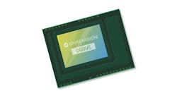
Will SPAD Become the New Go-To Image Sensor?
Key Highlights
- The technology may improve imaging in low light, bright light, and rapidly changing conditions.
- Applications include robotics, vehicles, drones, LiDAR, and inspection of reflective parts.
- SPAD can reduce motion blur and vibration effects, potentially simplifying downstream perception.
- Cost and processing requirements have been challenges, though commercial products are beginning to emerge.
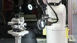
As machine vision systems take on increasingly complex tasks, the demand for sensors that can see more, measure faster, and perform in challenging lighting conditions continues to grow. One technology that’s starting to attract attention is the single-photon avalanche diode, or SPAD.
SPAD has been in existence since the 1960s. However, it has only been in the last 15 to 20 years that SPAD has become more commercially viable.
Sebastian Bauer, CEO of Ubicept, believes SPAD will soon become the go-to image sensor technology for machine vision and industrial imaging applications. In fact, Bauer so strongly believes in SPAD that he and several other MIT and University of Wisconsin scientists founded Ubicept, a company that specializes in SPAD.
What is SPAD Technology?
SPAD technology enables image sensors to detect individual photons, the smallest units of light, and precisely measure their arrival times. Essentially, SPAD detects individual photons by operating sensor pixels in a highly sensitive mode that triggers an electrical pulse whenever a photon arrives. Because SPAD sensors can count photons and precisely measure their arrival times, they are well suited for applications such as LiDAR, depth sensing, 3D imaging, and low-light imaging.
But SPAD can also be very effective in bright-light environments as well, provided the image processing is done correctly, Bauer says. Indeed, SPAD technology, if it can be scaled, is capable of bringing significant advancement for imaging in a wide range of applications, such as inspection of shiny or reflective objects.
“We kind of saw the writing on the wall that single photon sensors, at least when you do the processing the best way possible, could replace conventional image sensors,” Bauer says.
SPAD detects individual photons by operating sensor pixels in a highly sensitive mode that triggers an electrical pulse whenever a photon arrives.
How Does SPAD Differ from CMOS?
Conventional complementary metal oxide semiconductor (CMOS) image sensing technologies measure how much light arrives at each pixel, rather than detecting the arrival of an individual photon. In a conventional CMOS image sensor, each pixel converts incoming light into an electrical signal that is processed by circuitry integrated directly on the sensor chip.
In the earlier days of commercial image sensing, the conventional CMOS technology became dominant because it was commercially economical to produce chips that provided low power consumption, high resolution imaging, and increasing levels of on-chip integration. However, as LiDAR, 3D imaging, and various time of flight applications became more common, CMOS-integrated SPAD sensors became more economically viable.
How and Where Does SPAD Perform Better?
Broadly speaking, SPAD excels on a moving platform in extremely low light or extremely bright light environments, Bauer says.
“I think SPAD sensors really shine in use cases where you have anything that moves and has a camera on it,” Bauer says. “So I'm talking about a camera for driver assistance systems, backup cameras for cars, driver assistance systems. I'm talking about robots. I'm talking about drones, helicopters, planes.”
Conventional image sensors, such as CMOS, can struggle with motion blur, low-light conditions, and rapidly changing lighting environments, which often means a manufacturer—a drone manufacturer, for example—might need to add an extra layer of sensor technology such as LiDAR or thermal imaging. But SPAD sensors can deliver high-quality perception in those types of environments and conditions from a single sensor, he says.
“So, if you had the highest camera perception level possible, you could probably start getting rid of these devices,” Bauer says.
Because SPAD sensors can count photons and precisely measure their arrival times, they are well suited for applications such as LiDAR, depth sensing, 3D imaging, and low-light imaging.
Another potentially valuable use for SPAD could be in harsh industrial environments that experience rapidly changing lighting conditions, Bauer says. Because SPAD sensors offer significant low-light sensitivity as well as very high dynamic range, they can capture image details across a broad range of lighting conditions without having to rely so much on auto-exposure adjustments, which is challenging for CMOS sensors. This is especially useful for such machine vision tasks as inspecting shiny/reflective parts, Bauer says.
“When you’re talking about shiny parts inspection, where sometimes the part reflects the light into the camera, it’s very bright and then it turns slightly and the light is reflected in a different direction, you have a dim lighting problem, a dimly lit scene,” Bauer says. “But SPADs don’t really struggle with that. I think that is super exciting.”
And, because SPAD sensors minimize motion blur and are less affected by physical vibration, improving image quality and simplifying downstream image-processing and perception tasks becomes less complicated—and ultimately less expensive—to achieve, he says.
Challenges of SPAD Technology
While Bauer says he is excited about the future, he notes that SPAD is a relatively new technology on the market compared to conventional CMOS imaging.
“I think it’s important to get it out in front of customers, let them see how it works, experience the quality,” he says.
Currently, SPAD systems can cost more than conventional CMOS systems, in large part because they often require larger and more sophisticated data processing systems to convert photon events into usable images, he says.
...as these sensors become available, they can be manufactured almost at the same price point of conventional image sensors.
- Sebastian Bauer
Nonetheless, a wide variety of use cases are already in place and products are being introduced to the market. To wit, Canon recently rolled out a 1 MPixel single photon sensor camera. Bauer says he expects more will follow, especially as other advancements, such as those occurring in AI, make it easier to scale applications.
“It’s a little undefined yet where exactly these sensors will be used and at what scale,” he says. “But I think we will see much more coming in the next 1 to 3 years. What many people haven't understood yet is that as these sensors become available, they can be manufactured almost at the same price point of conventional image sensors. I think we will see these applications pretty soon.”
For example, he notes that iPads are already deployed for medical imaging, fluorescence, lifetime imaging microscopy, and other such applications that simply weren’t available just a few years ago.
About the Author
 Jim Tatum
Senior Editor
VSD Senior Editor Jim Tatum has more than 25 years experience in print and digital journalism, covering business/industry/economic development issues, regional and local government/regulatory issues, and more. In 2019, he transitioned from newspapers to business media full time, joining VSD in 2023.