How FPGAs are used in embedded vision applications
Apurva Peri
With the emergence of high-resolution, bandwidth-hungry surveillance equipment, artificial intelligence integration, real-time analytics, and the rapid rise in Internet of Things (IoT) adoption, there’s been increased focus on edge computing for video data processing workloads. While edge computing offers such benefits as improved response time, optimized bandwidth budgets, and data privacy, it also poses complex challenges such as data and design security, and restricted power and footprint budgets. These constraints demand the need for specialized computing hardware with advanced security features.
Mid-range field programmable gate arrays (FPGA) can be defined as those with a logic density count in the range of 100K to 500K as compared to higher density FPGAs with logic densities ranging from 1M to 9M. High-range FPGAs are popularly used in applications such as advanced driver-assistance systems and data centers, while mid-range FPGAs deploy into a variety of embedded applications such as surveillance, gateway deices, small cell wireless applications, medical and industrial imaging, and unmanned aerial vehicle (UAV) monitoring.
The roles of FGPAs in technology evolution
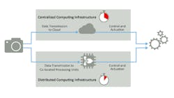
Edge computing is distributed computing that compared to centralized computing, can improve response time and conserve bandwidth by bringing computation and data storage closer to the application. With the ever-burgeoning IoT, an increasing number of commercial and industrial applications rely on the connected web of sensor-based, digital, and mechanical machines to monitor and control tasks. Wireless-enabled embedded systems, real-time analytics, and machine learning inference sit at the core of IoT.
A centralized storage and computation model does not offer an optimal approach for such applications, however, since these involve transmitting data to a central cloud server for processing and back to the devices for actuation. Edge computing addresses this by making compute resources available close to the data sources (Figure 1).
Related: CPUs, GPUs, and FPGAs: How to choose the best method for your machine vision application
Edge computing has its intricacies and constraints, however, as it demands accelerated computational performance with accurate and predictable outcomes, and strict power and footprint budgets. These limitations become especially complex when the applications involve embedded vision, since they require increased thermal head room, higher resolution with multiple 4K/8K channels supported by batteries, and often integrate artificial Intelligence and machine learning capabilities.
Having an efficient edge computing system for smart vision systems requires flexible hardware that can support multiple interfaces for sensors such as MIPI and SLVS and transport including HDMI, HDCP, USB, and SDI with advanced image processing capabilities that allow for protocol conversions, filtering, edge and depth detection at less than 5W power consumption. Owing to their accelerated processing, reconfigurability, and energy efficiency at optimal cost, FPGAs present a cost-optimized and powerful platform suitable for meeting edge computing requirements for embedded vision systems.
Compute horsepower and power efficiency
Logic elements, an array of digital signal processing (DSP) interlocked with memory blocks, comprise the building blocks of an FPGA. Intrinsically parallel and well suited for specialized tasks that demand extensive parallelism during processing, hardware-programmable FPGAs accelerate the convolutional neural network (CNN) used for object detection and identification and other computer vision applications. FPGAs offer larger DSP capabilities than most CPUs and obviate the need for using external DSP elements, reducing total cost for a given functionality. Additionally, by interlinking memory with the core computing units in a distributed fashion, FPGAs bring processing closer to memory which contributes to optimized power utilization.
Edge devices may be deployed in remote locations with limited human access, and/or may require an uninterrupted power supply for critical applications such as aerial vision, medical vision, traffic monitoring, and other such automated processes. Even if a solution can offer high-performance in a small footprint, it may not necessarily be power-efficient.
FPGAs offer up to 30% lower power dissipation in vision-based machine learning applications as opposed to CPUs that work with a GPU. For a comparable throughput, FPGAs enhance thermal stability and optimize cooling costs. Devices based on non-volatile Flash/SONOS technology that feature transceivers architecturally-optimized for mid-bandwidth applications inherently provide the necessary power efficiency.
Related: MIPI CSI-2 interface provides flexibility for next-generation embedded vision systems
Customization and time to market
Flexibility represents a more obvious benefit of deploying FPGAs in vision-based machine learning devices for three reasons. First, FPGAs integrate numerous diverse resources into one chipset such as hard and soft IP cores for camera sensor interfaces, control logic, compression algorithms, display and network interfaces, and an architecture favorable for neural network architectures. Second, by definition, FPGAs can be programmed either in part or whole while in the field. For example, if a developer were to update a deployed application system to latest versions of HDMI, MIPI CSI or even USB, it would be easier to do so on an FPGA than a custom built ASIC. It empowers one to build future-proof, scalable designs, conform to evolving standards, and reconfigure hardware for revised specifications.
If a MIPI-based image processing system necessitates an upgrade to support additional camera sensor interfaces, an FPGA can implement such a change with no modification to the system. This affords notable cost and time advantages. Furthermore, FPGAs are also scalable - if an algorithm or a function gets larger, FPGAs can be efficiently daisy-chained to adapt to the code.
Implementation challenges and requirements
While FPGAs represent a suitable option for the implementation of AI/ML-based functions at the edge, designing with an FPGA can be daunting and poses challenges especially for someone without prior FPGA experience.
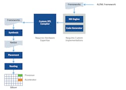
A typical design flow involves working with one of the many available ML platforms to source tools, libraries, and resources to build a framework for a neural network and generate the associated code (Figure 2). The code compiles using a custom register transfer level (RTL) compiler followed by the traditional FPGA design flow of RTL synthesis, netlist generation, and place and route. FPGA’s programming model is inconsistent with the larger software development community. Although a wide range of platforms to develop an ML framework exist, each offers a unique design structure and requires custom implementation, and there’s limited availability of application-specific evaluation platforms with an easy out-of-the-box experience in the FPGA industry. Investing in hardware to validate a CNN—particularly when evaluating multiple platforms to determine the optimal option—also becomes imperative.
A software developer with no FPGA experience must be able to program a trained neural network on a hardware-free evaluation and validation platform, with access to multiple OS support. Meeting the programming challenges on FPGAs tailored around machine learning applications requires a unique combination of techniques and design flows. Such a combination must offer an extensive range of interoperable frameworks and abstracts hardware programming by allowing developers to code in C/C++ and use power-efficient neural networks.

One example of this approach can be seen in the software development kit (SDK) that Microchip (Chandler, AZ, USA: www.microchip.com) offers with its PolarFire FPGAs (Figure 3). Such kits enable the development of low-power, flexible overlay-based neural network applications without having to learn an FPGA design flow. Kits that include a bit-accurate simulator enable users to validate the accuracy of the hardware while in the software environment. Kits should ideally also include neural network IP so that different network models can be loaded at run time and should also provide the flexibility to port multi-framework and multi-network solutions.
Related: Deep learning chip enables efficient device processing
Security and reliability considerations must be made to ensure authentic, tamper-proof, and safe inference—particularly in applications like surveillance or drones. Updating the FPGA in real-time provides a fundamental advantage because susceptibilities can be addressed with new definitions. The FPGA must present competitive security features to ensure full design IP protection, secure data communications, and anti-tamper capabilities.
In an embedded vision scenario, deep learning inference schemes are typically part of a broader system that integrates camera sensor interfaces like MIPI and SLVS, an image signal processing unit, and transport interfaces like CoaXPress, HDMI, 10GigE Vision, SDI, and wireless connectivity. An ideally-suited FPGA for such applications should be able to seamlessly support and integrate diverse protocols and interfaces with minimal developer effort as part of a total system solution.
Decentralized edge computing has gained popularity to overcome the shortcomings of long latency and bring compute resources closer to data sources. For embedded vision applications such as auto-piloting vehicles, surveillance, and medical imaging; cost-optimized mid-range FPGAs combine high-performance, design flexibility and energy-efficiency. While the complex programming models extend a significant challenge to the adoption of FPGAs, there has been an extensive effort from FPGA vendors to overcome traditional FPGA design flow challenges and bridge the gap to enable the creation of low-power FPGA-based embedded vision systems.
Apurva Peri is a Senior Engineer, Product Marketing, at Microchip (Chandler, AZ, USA: www.microchip.com)