Backside-illuminated image sensors: Optimizing manufacturing for a sensitivity payoff
By Jan Provoost and Piet De Moor, imec
Backside-illuminated CMOS image sensors (BSI) capture light directly on the silicon light-sensitive layer. They have a higher sensitivity in a broader spectrum than the mainstream frontside-illuminated imagers (FSI). And in the field of high-end and specialty imagers, they have started to compete with established charged-coupled device (CCD) technology.
BSIs, however, are more difficult to fabricate than FSIs. They require advanced wafer thinning, surface passivation techniques to maximize sensitivity, and careful substrate engineering to minimize crosstalk. Using the possibilities of BSI technology, imager researchers are also looking at alternative architectures, producing pixels and readout electronics as separate dies and stacking those using high-density microbumps and TSVs.
Detecting and capturing light with image sensors: CCD versus CMOS
Silicon is an ideal material to make image capturing sensors, for use in digital cameras and other products. It absorbs that part of the electromagnetic spectrum that -- through a lucky quirk of nature -- matches the light that is visible with our eyes.
The first commercial sensor chips were CCDs, appearing around 1985. By the early 1990s, the CMOS process was well-established and CMOS imagers started to appear, first for low-end imaging applications or low-resolution high-end applications. Since then, the market has split into two segments. For low-cost, high-volume imagers, CMOS imagers have clearly overtaken CCDs. In high-performance, low-volume applications, CMOS and CCD imagers share the market, mainly because CCD technology still allows for a lower noise. In total, in 2010, the market share of CMOS imagers was 58% vs CCDs; this share is forecast to grow to 66% in 2015.1
When light strikes a CCD pixel sensor, it is stored as a small electrical charge. Next, these pixel charges are transported, one at a time, to the output stages. And only then, on a separate chip, are the voltages converted to the digital domain, to bits. A CMOS imaging chip, on the other hand, is an active pixel sensor: each pixel has its own circuitry. CMOS image sensors are fabricated using standard CMOS production processes, so they require less-specialized manufacturing facilities than CCDs. Also, they consume less energy, are faster, are better scalable, and allow integrating on-chip image processing electronics.
The roadmap in the image sensor industry is mostly concerned with decreasing price per pixel while increasing the number of pixels on a given chip surface -- reducing the pixel pitch. Currently, high-volume sensor production capacity is moving from 200mm fabs to 300mm fabs, with minimum features reaching 65nm, and resolutions pushing beyond 16 megapixels.1
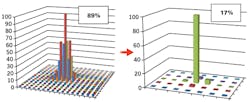
But next to this, R&D centers such as imec are also concerned with improving the image quality. Not so much looking for smaller pixels, but for optimal performance. Capturing more photons (improving the quantum efficiency, QE), capturing them in the correct pixels (reducing or eliminating the crosstalk), and capturing a larger part of the light spectrum. Solutions are used in specialty imagers, e.g. for space applications (Figure 1).
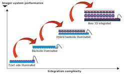
From frontside- to backside-illuminated CMOS sensors
Mainstream CMOS imaging chips consist of a photoactive layer with CMOS circuitry (the pixel transistors and image processing circuitry), with the metal interconnect layers on top. Installed in a camera, the light will first pass a lens, then the chip’s interconnects, and only then hit the light-capturing layer. This of course means that the wiring will reflect and absorb part of the light, attenuating the signal that is available to be captured. Such an image sensor is frontside-illuminated (FSI), i.e. the light falls on what we conventionally see as the front of the chip. Without special measures, the quantum efficiency (QE) will be less than 50% over a limited spectrum. Typical solutions to overcome this involve using microlenses, sometimes in combination with light pipes, to guide the light around the metal interconnect. In this way, the efficiency may improve, going up to 80%, but with little improvement in the spectrum coverage.
In a back-illuminated (BSI) sensor, the chip is turned upside down, with the light falling on the backside. In the fabrication process, after the CMOS circuitry and the interconnect layers have been created, the backside of the chip is ground and etched away until the photoactive layer is exposed. The resulting chip is very thin, sometimes below 5µm. When carefully engineered, such a sensor can improve the chance of capturing an input photon to over 90%. It will also be sensitive over a wider spectrum than is possible with FSI sensors, having a good efficiency even into the ultraviolet bands.
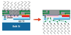
The process to thin the BSI wafer to expose the photoactive layer is not trivial. The entire wafer has to be thinned extremely uniformly and precisely, just exposing -- but not damaging -- the photo-active layer. In addition, this remaining layer has to be defect-free and have a uniform thickness, to enable uniform light sensitivity. The resulting thinness also introduces major wafer handling issues. Because of the additional costs and yield issues, BSI sensors were at first used only in niche applications, where a superior low-light performance was important and price was not the first concern.
In 2007, OmniVision Technologies was the first to perfect a fabrication process for BSI imagers. Sony then introduced new photo diode materials and processes that allowed them to present the first consumer BSI sensor in 2009. Competitors followed suit, and in 2010 back-illumination came to the mass-consumer market when Apple included a 5Mpx OmniVision detector in the iPhone 4.
Playing with the relation between efficiency, noise, and the active layer
In an image sensor, light photons hitting the photoactive layer are absorbed; their energy is converted into electron-hole pairs. But the thickness of the photoactive layer needed to absorb light increases with the wavelength. So to capture a broader spectrum including red and infrared, a thicker active layer is needed. In typical FSIs, the layer in which absorption and collection takes place is only a few micrometers thick. Charges from longer-wavelength light that are absorbed deeper recombine in the low-resistive and defect-rich substrate long before they reach the collecting diode junctions. While in principle silicon is able to detect light of wavelengths up to 1100-1200nm (infrared), these substrates will only detect light up to around 600nm.
These sensitivity issues can be tackled in BSIs. The sensitivity towards the red and infrared bands can be optimized through a careful design of a thick highly-resistive epitaxial layer. And sensitivity in the short-wavelength spectrum can be enabled by making the surface passivation layer as thin as possible. Such a passivation layer can be created with a high-dose implant and laser annealing. In this layer, carriers immediately recombine, so it is not light-sensitive. Therefore, if we want to avoid losing sensitivity in the blue spectrum, it should be as thin as possible.
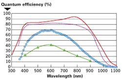
With such a layer, optimized for both ends of the visible spectrum, we were able to make a BSI imager with a record efficiency over a broad spectrum. In the full visible light spectrum (400-800nm), the efficiency is fairly constant between 80 and 90%. And even in the infrared, at 850nm, the efficiency is still 80%.
Next to the sensitivity issue, there is a second quality consideration: The electron-hole pairs caused by the incoming photons should be collected in the correct image pixel circuit before they recombine. This is not straightforward, as the electron-hole pairs will diffuse in all directions, sometimes so far that they are collected by neighboring pixels. This effect, commonly termed crosstalk, reduces the sharpness of the images captured with these sensors.
For our record BSI sensor, we grew high-quality EPI layers on standard silicon. By tuning the growth conditions, it is possible to engineer specific doping profiles in the detection layer. This way, a built-in electric field can be created to pull the generated carriers from the substrate to the diode at the surface, where they are collected, largely avoiding crosstalk.
Another technique that we experimented with is to separate the pixels with deep and narrow trenches filled with highly doped polysilicon. This creates a built-in electric field at the sides of the trench, effectively creating a wall between the pixels and eliminating crosstalk. One obvious disadvantage of this method is that you lose part of the detection surface, i.e. the fill factor will slightly decrease.
Absorbing light with the backside of the sensor offers many advantages. But the backside thinning must be extremely uniform to have a uniform spectrum sensitivity over the sensor. At imec’s fab, we’ve been able to thin wafers down to 12µm. The best uniformity that can be reached is <2µm thickness variability on 200mm wafers. In addition, the thinned-down substrate should be damage-free, as each irregularity in the silicon crystal will be a catalyst for recombinations, and thus reduce the efficiency. And last, we need a carefully chosen antireflection layer, with a maximum response to the spectrum that the sensor needs to detect.
Future developments with BSI imagers
Almost all CMOS image sensors are fabricated monolithically: the light-capturing layer and the readout electronics are made on the same substrate. Monolithic FSIs and BSIs cover most of the current needs in the imaging market. But to improve the imager quality and extend its possibilities, other architectures are also possible.
One step up are hybrid BSI sensors, where you separate the light capturing layer and the readout electronics in 2 layers connected face-to-face through microbumps.
The advantages for hybrid sensors are that both layers can be designed and optimized independently. A photosensitive layer can have a layer other than silicon, e.g. InGaAs, CdTe, or (Al)GaN, to capture specific light spectra. Imec designed a sensor for the European Space Agency for monitoring the solar activity from space. It was made with a separate AlGaN Schottky diode array, making it a solar blind (E)UV sensor: it captures ultraviolet light, but not the visible spectrum. A second advantage of hybrid designs is that different CMOS technology generations can be used for both layers.
An obvious disadvantage is that the pixel size scaling is limited to how small and dense the microbumps can be made. Imec researched microbumps using indium and copper/tin (CuSn). Using indium bumps, we were able to make sensors with a 20µm pitch, and work has started on 10µm pitches. Indium microbumps are valuable in cryogenic applications, for example the solar blind (E)UV sensor. CuSn microbumps, down to a pitch of 20µm, offer even better process control, and will probably prove the best option for non-specialty applications. Our current way to bond the two layers is through die-to-die thermocompression.
As a next step, we see 3D integrated image sensors, where you stack 3 or more layers, connected with through-silicon vias (TSVs). These will allow integrating dedicated, optimized layers in the sensors. These layers can be additional electronics to add intelligence and to further process the image that is captured. Or it could be an additional optical layer, to precondition the light that hits the sensor. Next to the advantages of flexible integration, these designs also offer a much increased speed, allowing a massive parallel processing of all pixels through the various layers.
Conclusion
Backside-illuminated imagers offer a number of advantages over frontside-illuminated sensors. As the extra processing challenges have been overcome, they have started to appear in mass-market and even in high-end products. But BSI imager designs are also extendible for specialty applications. They have the potential for a higher sensitivity over a wider spectrum. And as they get integrated in hybrid two-layer, or even multi-layer designs, they can be the driver for a whole array of new vision applications.
REFERENCES
1. IC Insights Research Bulletin, CMOS Image Sensors Regaining Growth Momentum, May 10, 2011-10-13.
2. Y. Bai et al., Teledyne Imaging Sensors: silicon CMOS imaging technologies for x-ray, UV, visible, and near infrared, SPIE proceedings Vol. 7021, 2008.
3. K. De Munck, K. Minoglou, P. De Moor, "Thinned Backside-Illuminated Imagers," in Burghartz, Joachim (Ed.), Ultra-thin Chip Technology and Applications, Springer 2011.
Piet De Moor, R&D team leader, heterogeneous integration at imec. After obtaining his PhD degree in Physics from Leuven University, Piet De Moor joined imec in 1998. First he was involved in research and development of MEMS-based infrared detector systems and MEMS packaging at wafer level. Next, he headed a team developing 3D integration technology, including wafer thinning, through-Si via processing and high density bumping. His current research focus is advanced CMOS imagers such as backside-illuminated and hybrid imagers suitable for high-end imaging applications.
Jan Provoost, science editor at imec, is responsible for communicating imec’s technology programs and activities to the global media and serving as editor and co-author of technical documentation. He obtained his M.A. in languages in 1989 and his M.Sc. in information science in 1993, both from the Catholic University of Leuven, Belgium. Contact the authors at [email protected].
- Republished with permission from Solid State Technology, Nov. 11, 2011.